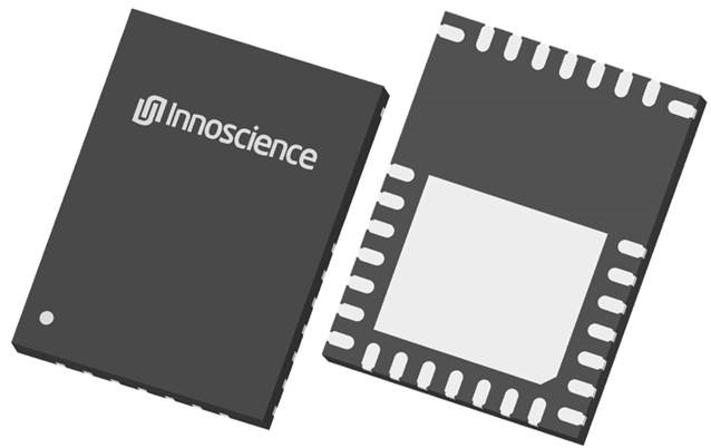
Innoscience‘s family of 700V integrated devices available from Richardson RFPD combine power GaN HEMT, driver, current sense and other functions within a single, industry-standard QFN 6x8mm package.
The 700V ISG610x SolidGaN™ devices cover the Rds(on) range from 100mΩ typical (140mΩ max) to 320mΩ typical (450mΩ max), saving PCB space and BOM count, while increasing efficiency and simplifying design for applications including USB-PD chargers, LED lighting, and AC/DC power supplies and PFC, QR flyback, ACF, and LLC converters.


ISG610X - High-Performance SolidGaN™
The ISG610X is a high-performance SolidGaN™ IC integrating a 700V E-Mode GaN FET with a high-voltage linear regulator, a smart gate driver, and an accurate loss-less current sense circuit. The high-voltage linear regulator with up to 80V input capability eliminates the need for external voltage regulators and maintains tightly regulated 6V gate drive voltage for the integrated GaN FET. The integrated smart gate driver provides a dual slew-rate gate driving scheme while adjusting the gate turn-on slew rate to achieve high frequency operation, high power efficiency, and low EMI performance. The loss-less current sense circuit eliminates external current sense resistors and increases system power efficiency.
The ISG610X provides an autonomous standby mode with a smooth transition and minimizes the quiescent current at no load condition. Additional features include 5V LDO supplying external digital isolators, UVLO, OCP, and OTP protection. Its operation is best understood by referring to the Functional Block Diagram.
- Hover to Learn More

