Electric Vehicles Fast Chargers
Introduction
Electric Vehicles (EV) need Direct Current (DC) to charge the Lithium Ion batteries that are within the vehicle. Faster charging speeds enable vehicle owners to spend less time at a charging station and more time getting to their final destination, whether it be work, home, or a long trip for a vacation. Power designers have developed some really good designs to achieve the fastest charge rates within safety standards.
To design a good fast charging system for EVs we need to first minimize the cooling effort, deliver high power density, and reduce overall system size and weight especially in onboard charging systems. High power density will also require the need for forced air cooling. Using WBG devices will most definitely reduce charging times with the use of Gallium Nitride (GaN) or Silicon Carbide (SiC) devices which are best at achieving high power density in the design architecture.
WBG Advantages
WBG power devices like SiC are able to block very high DC link voltages with lower losses as compared to Silicon (Si) insulated gate bipolar transistors (IGBTs). The power converter can operate at a higher voltage, thereby reducing the amount of current for the required power transfer. Reduced current directly leads to less copper usage, which in turn increases the power density. Figure 1.
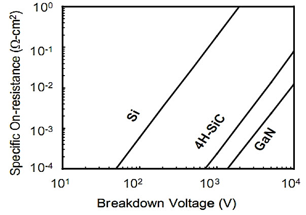
Figure 1: Central (or string) inverters, microinverters and power optimizers. (Courtesy of solartribune.com)
WBG Advantages
First, let’s look at the design of a conventional on-board, fast-charging architecture, with a two-stage design, containing a Power Factor Correction (PFC) stage on the front-end followed by an isolated DC/DC converter. Figure 2.
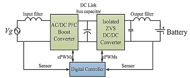
Figure 2: A conventional on-board EV charger (Image from Reference 1))
Using Wide BandGap (WBG) devices, like SiC and GaN, enable EV chargers to operate with lower losses and higher efficiency than Si, enabling less generated heat which leads to less substantial and less costly thermal management; WBG devices have higher breakdown voltage as well (See Figure 1). Discrete SiC MOSFETs are commercially available 650V-700V, 900V, 1000V, 1200V, 1700V while GaN transistors operate up to 650V. Since WBG materials will withstand higher operating temperatures, and have lower leakage currents as well as lower thermal resistance, these devices will handle more power in a given footprint than Si.
Today’s battery voltages in Electric Vehicles are typically 200V to 800V+, so GaN will capably handle less than 500V for safe design practice taking into account switching transients and SiC will easily handle the higher end voltages.
In addition to the lower heat generated by the reduced switching losses, SiC devices have a higher thermal conductivity than Si (4.9 W/cm-K for SiC, as opposed to 1.5 W/cm-K for Si). Therefore, heat is more easily transferred out of the SiC device, and thus the device temperature increase is slower; GaN has a lower thermal conductivity than Si; however, the superior switching loss performance of GaN far outweigh that of Si in this fast charging application as we will see in the paragraphs below.
Fast switching capabilities result in lower switching losses. Lower switching losses reduce heat generated during the switching process and increase efficiency. Less heat generated can lead to smaller, less expensive thermal management solutions. Operating at higher frequencies can also enable the use of smaller, less expensive passive energy storage components like inductors and capacitors. GaN is far superior than SiC or Si regarding switching losses.
However, switching losses don’t tell the full story. Total losses include switching and conduction losses. Switching losses are those generated when the device “switches” from the off-to-on or on-to-off state. Conduction losses occur when the device is fully on; the primary contributor to conduction losses is Rds(on) or (Resistance from drain to source in the “on” state). In general, SiC devices have a lower, more stable Rds(on) over temperature than GaN devices. This can lead to lower conduction losses for SiC compared to GaN.
Gauging overall losses
Figure of Merit (FOM) is used as a general comparison of both switching and conduction losses and is calculated by (gate charge * on-resistance) or (Qg * Rds(on)). The gate charge (Qg) is an indicator of switching losses while the Rds(on) represents conduction losses. Comparing the product of the two parameters gives an indication of overall performance capabilities.
GaN devices have a FOM 13x better than the best Si super junction MOSFETs primarily due to the very low gate charge.
WBG Key Features vs Si
SiC, as well as GaN, operate at higher frequencies than Silicon MOSFETs or IGBTs. WBG devices will have far less switch power losses than Si as well. WBG higher switching speed also shrinks larger, heavier magnetics, thus enabling lighter, smaller power designs, with better energy efficiency.
SiC devices will withstand higher temperatures than GaN, thus reducing cooling needs, but GaN has a lower-threshold gate voltage than SiC to attain the required output current. GaN also has a higher rate of voltage change with respect to time (dv/dt) and hence faster switching in both on and off periods than SiC, thus enabling higher speeds.
Fast On-Board Chargers (OBC) Using GaN
GaN has high power density and very fast switching capabilities which makes it the power device of choice over Si and SiC for fast on-board chargers under 600V. Reduced switching losses and higher efficiency enable GaN to dissipate less heat, thus requiring smaller, less expensive heat sinks.
These features lead to a smaller, lighter on-board charger which is advantageous to maintain a lower automobile weight and size. GaN can support the million hour MTTF reliability benchmark at a junction temperature of 200°C or higher.
GaN compared to Si: Size, efficiency and weight are important for OBC.
- 4 x smaller (1/4 the size)
- 4 x lighter (1/4 the weight)
- 4 x efficiency (1/4 the efficiency loss)
SiC devices will begin to take over as the charger voltages approach 600V to 1kV+ ranges because of their higher breakdown voltages, ruggedness, fast switching and higher power capability. Silicon loses the battle here as well.
Fast Off-Board Chargers Using SiC
Typically, a transformer is needed to reduce high voltages from the line; however, with SiC devices (at higher voltages above 600V allowing smaller cable sizes and less heat), the voltage would not need to be stepped down, allowing electricity to be used right off the line. The off-board charger is served by a three-phase AC circuit at 208, 240, 380, 480, or 575 V. SiC shines in these higher voltage, fast off-board chargers which convert the external AC to DC power at greater than 93% efficiency.
A DC charger with 150kW can put a 200 km charge on a battery in just 15 minutes. Again here, SiC wins the battle as a fast off-board charger because the cables from the charger to the EV will be smaller and lighter and SiC can handle the external AC to higher voltage DC conversion.
Higher Charging Power Design
Designers can achieve higher charging power, for example 2.4kVAC/50 kW, by using ten 230VAC/7.2kW charging modules connected in series at the input side and in parallel at the output sides. This architecture, with GaN HEMT devices, provides high-power density, high-efficiency and high-power simultaneously. Zero-voltage switching, for fast-charging, should be implemented. Figure 3.
See more details regarding this design architecture in Reference 1.
In summary, we can see that GaN and SiC are the prime power element choices for electric vehicle fast charging design architectures.
Proper PC board layout and gate-drive parameter design enable GaN and SiC power devices to revolutionize EV charger capabilities and help to make fast EV charging a reality.
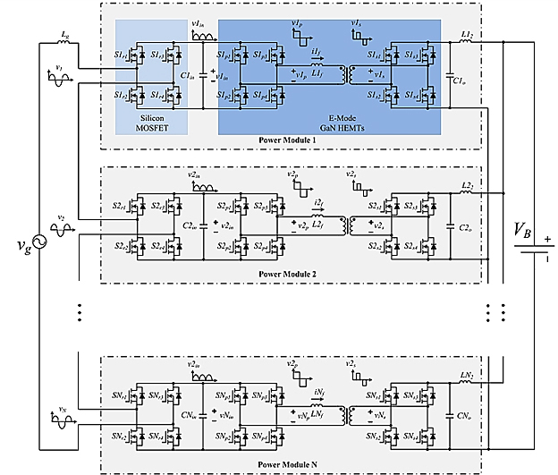
Figure 3: Input-series-output-parallel (ISOP) ultrafast matrix converter charger design architectures, using GaN HEMT devices, need no bulky DC link capacitors and have high efficiency (Image from Reference 1)
References
- H. Naik, “4H-SiC Lateral MOSFETs on (0001), (000-1) and (11-20) oriented SiC substrates” Master’s Thesis, Rensselaer Polytechnic Institute, Troy, NY, 2009. (This may be behind the IEEE Xplore pay firewall)
- Comparison of Wide Bandgap Semiconductors for Power Applications, B. Ozpineci, L.M. Tolbert, S.K. Islam, M. Chinthavali, Oak Ridge Laboratory
